This mini-board was designed by Jeff Brown to get better control on the TI-99/4A interrupts system. Basically, it doubles each interrupt with a non-maskable LOAD* interrupt. Since LOAD* causes a branch into the high-memory expansion, you can have a program there that will handle interrupts better than the console ROMs. A spare CRU bit in the console lets you turn this feature on and off.
A bit of theory
Hardware description
Building the board
Installing the board
Software
There are two kinds of interrupts with the TMS9900: maskable and non-maskable interrupts. Non-maskable interrupts are triggered by bringing the LOAD* pin low. As the name implies, they are not maskable, which means the TMS9900 has to answer immediately. It does so by performing an implied BLWP @>FFFC.
Maskable interrupts are more sophisticated. They are arranged in 16 levels of priority, with 0 (the reset interrupt) having the highest priority. Such interrupts are signaled by grounding the INTREQ* pin of the TMS9900, while placing the level number on pins IC0 through IC3. This is achieved by an independent chip, typically a TMS9901, that receives interrupts from 16 different pins, places the proper code on IC0-IC3, and brings the INTREQ* line low. Software instructions such as LIMI let you decide upon a threashold level: interrupts with a higher priority (lower number) will be answered, others will be ignored. The TMS9900 answered this kind of interrupts by performing an implied BLWP to an address that depends on the interrupt level: >0000 for level 0, >0004 for level 1, >0008 for level 2, etc. In addition, it bumps up the current interrupt mask so that only interrupts with a higher priority will be accepted, until the interrupt service routine returns.
That's a wonderful and sophisticated way to handle interrupts, unfortunately it's not how things happen in the TI-99/4A. First of all, the IC0-IC3 pins were hard-wired so that all interrupts are read as level 1. Furthermore, the TMS9901 in the console is wired in such a way that only 3 interrupt levels can be used: level 1 for peripheral cards, level 2 for the videoprocessor, level 3 for the TMS9901 internal timer. To add insult to injury, the interrupt service routine in the console ROMs does not handle level 3 properly, in that it either considers that all interrupts are level 3 or that none are, but does not check the TMS9901 to see what the actual level is! On top of that, it looses the return address when handling level 3 interrupts!
One way around this unfortunate situation would be to replace the console ROMs with EEPROMs, so we can modify the interrupt service routine, and to connect the IC0-IC3 pins as they should be. Jeff Brown came up with another solution: he designed a small module to be installed inside the console, that will generate a non-maskable LOAD* interrupt each time a maskable interrupt occurs.
This very simple module consists in only 3 TTL chips (more precisely, 2 and 1/4): two 74LS00 quad-NAND gates, and one 74LS74 dual flip-flop.
TMS9901 +5V---WWW---+------------------, 74LS74 |
The INTREQ* pin is normally used by the TMS9901 to signal a maskable interrupt to the TMS9900. Here, it is also inverted with a NAND gate mounted as an inverter, masked with the P0 pin and inverted again to be applied to the 74LS74 flip-flop.
P0 is one of the TMS9901 output pins left unused in the TI-99/4A console. It is normally low, but can be modified via CRU bit 16 (address >0020). When it is high, any low signal on INTREQ* will result is a high signal on the Clk input of the 74LS74.
The 74LS74 contains two flip-flops. When a Clk input goes high, the corresponding flip-flop copies the content of the D input to the Q output, and its opposite to the Q* output. The rest of the time, Q and Q* remain unchanged. A low level on Clr* resets Q as 0 and Q* as 1, whereas a low level or Set* does the opposite. Note that once the clock has ticked, is must become low again to generate another flipping by becoming high: simply staying high has no effect. In the modification that we are about to make, this means that interrupts will be edge-triggered (i.e. fire when the line becomes active) as opposed to the usual TI-99/4A way of level-triggered interrupts (where an active line keeps generating interrupts until it's reset).
Is our case, the raising signal on Clk will copy the Reset* line (which is normally high) on Q, which itself is connected to the D input of the second half of the 74LS74. This half is clocked by the IAQ pin from the TMS9900. This pin goes high when the TMS9900 is acquiring an instructions from the memory, as opposed to reading or writing data. Only at that point will the Q* output become low and trigger a LOAD* interrupts.
The Q* output, combined with Reset*, is fed back to the first haf of the 74LS74, which it resets: Q becomes low when either Reset* or Q* is low. At the next IAQ pulse, the LOAD* line will thus become high again. This means that the LOAD interrupt line will never stay active for more than one instruction. This is critical so that the TMS9900 does not lose the return address by performing several BLWP @>FFFC one after the other! For the module to generate another LOAD* interrupt, either P0 or INTREQ* must become low again. Typically, INTREQ* will be reset when the interrupt it asknowledge.
The Reset* line is briefly brought down at power-up time, and when a new cartridge is inserted. It goes to many chips in the console, including the TMS9900 and the TMS9901. In the later, the reset signal results in bringing P0 low, i.e. the interrupt modification will be off by default. The Reset* signal also resets both halfs of the 74LS74 through their Clr* pins. Finally, Reset* is fed to the D input of the first flip-flop so a high signal will not be latched by mistake upon power-up.
Building this board is a good project for beginners because it's extremely easy to do. Since the circuit is so simple, you don't need to actually etch a printed circuit board. You may use one of those pre-etched, perforated boards. In addition, you will need:
2 74LS00 (quad NAND gates)
1 74LS74 (dual flip-flop)
3 1 kilohm resistors
3 14-pin sockets (optional).
Decide how you're going to arrange the chips, then cut the board accordingly. The smaller, the better since it will have to fit inside the console, where space is limited.
Solder the chips or the sockets. Sockets make it easier to change a bad chip, but they also make the board a little thicker. It should fit under the console hood, though.
Here is an example of how to connect the chips together. You may opt for a slightly different arrangement, as long as you follow the above schematics.
               74LS00                            74LS00
            +---+--+---+                      +---+--+---+
INTREQ*--+--|1A     Vcc|             LOAD*----|1A     Vcc|
         '--|1B      4B|--,          RESET*---|1B      4B|--,
         ,--|1Y      4A|--+-------------------|1Y      4A|--+
         '--|2A      4Y|--------------,    ,--|2A      4Y|  |
P0----------|2B      3B|--,           |    +--|2B      3B|--+--WWW--+5V
         ,--|2Y      3A|--+           |    |  |2Y      3A|--'   1K
         |  |Gnd     3Y|--|--------,  |    |  |Gnd     3Y|
         |  +----------+  |        |  |    |  +----------+
         '----------------'        |  |    |
                                   |  |    '--WWW---+5V
       ,------------------------,  |  |        1K
       |     74LS74             |  |  |
       |  +---+--+---+          |  |  |
RESET*-|--|1Clr*  Vcc|          |  |  |
       '--|1D   2Clr*|----------|--|--'
IAQ-------|1Clk    2D|---RESET* |  |        All Vcc to +5V
        ,-|1PR*  2Clk|----------|--'        All Gnd to ground
        | |1Q    2PR*|--,       |
LOAD*---|-|1Q*     2Q|--|-------'
        | |Gnd    2Q*|  |
        | +----------+  |    1K
        '---------------+---WWW---+5V
Solder some length of wire to the pins that should lead to the TMS9900 (RESET*, LOAD* and IAQ) and to the TMS9901 (INTREQ* and P0). Also install longer wires, possibly of a different color, for the power supply (+5V and ground).
Once done, tape or glue the board on a piece of cardboard, or any kind of insulating material, so it wont make contact with the metal casing aroud the motherboard.
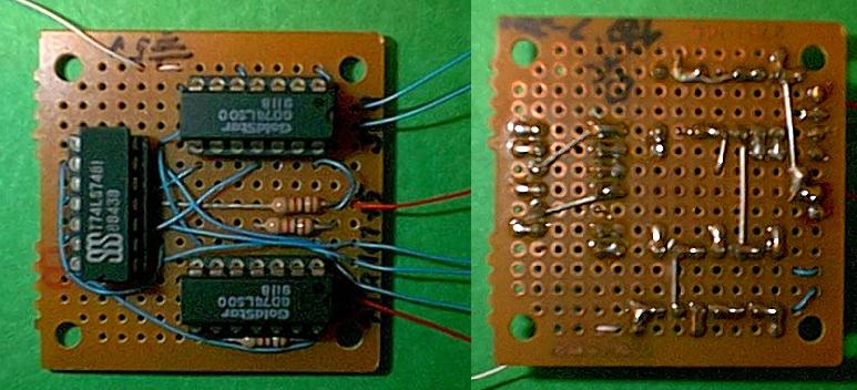
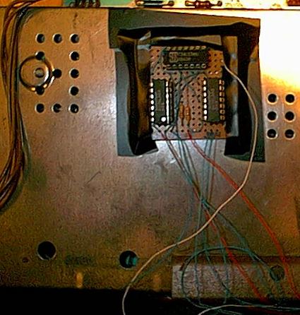
Here is a picture of a board that was made for me by Richard Bell.
To install this board, you must open your console. No big deal though. Refer to my console surgery page for detailed instructions.
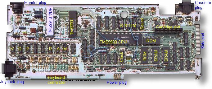
Identify the TMS9900: with 64 pins, it's the biggest chip on board. Then identify the TMS9901: it's the 40-pin chip that's the closest to the keyboard. Here is an annotated picture, to help you orient yourself. Notice that there is a notch on one end of each chip: this is where pin #1 is.
Now you must solder some wires from the board to both the TMS9900 and the TMS9901.
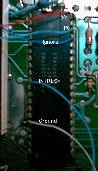
On the TMS9901, you want pin #11 (INTREQ*) and pin #38 (P0). Here is a picture (the wire labelled "ignore" is a different modification).
       +----+--+----+
 RST1* |1 o       40| Vcc
 CRUOUT|2         39| S0
 CRUCLK|3    T    38| P0
 CRUIN |4    M    37| P1
   CE* |5    S    36| S1
 INT6* |6         35| S2
 INT5* |7    9    34| INT7*/P15
 INT4* |8    9    33| INT8*/P14
 INT3* |9    0    32| INT9*/P13
  PHI* |10   1    31| INT10*/P12
INTREQ*|11        30| INT11*/P11
   IC3 |12        29| INT12*/P10
   IC2 |13        28| INT13*/P9
   IC1 |14        27| INT14*/P8
   IC0 |15        26| P2
   Vss |16        25| S3
 INT1* |17        24| S4
 INT2* |18        23| INT15*/P7
    P6 |19        22| P3
    P5 |20        21| P4
       +------------+
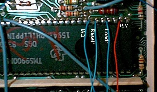
On the TMS9900, you want pin #4 (LOAD*), #6 (Reset*) and #7 (IAQ). Here is a picture.
        +----+-----+----+
    Vbb |1 o          64| HOLD*
    Vcc |2            63| MEMEN*
   WAIT |3      T     62| READY
  LOAD* |4      M     61| WE*
  HOLDA |5      S     60| CRUCLK
 RESET* |6            59| Vcc
    IAQ |7      9     58| nc
   PHI1 |8      9     57| nc
   PHI2 |9      0     56| D15
    A14 |10     0     55| D14
    A13 |11           54| D13
    A12 |12           53| D12
    A11 |13           52| D11
    A10 |14           51| D10
     A9 |15           50| D9
     A8 |16           49| D8
     A7 |17           48| D7
     A6 |18           47| D6
     A5 |19           46| D5
     A4 |20           45| D4
     A3 |21           44| D3
     A2 |22           43| D2
     A1 |23           42| D1
     A0 |24           41| D0
   PHI4 |25           40| Vss
    Vss |26           39| nc
    Vdd |27           38| nc
   PHI3 |28           37| nc
   DBIN |29           36| IC0
 CRUOUT |30           35| IC1
  CRUIN |31           34| IC2
INTREQ* |32           33| IC3
        +---------------+
You also need to find +5V and ground somewhere: pin #2 (Vcc) of the TMS9900 will provide you with +5V, pin #26 (Vss) with ground. Alternatively, you can take them from the TMS9901: Vcc is pin #40, ground is pin #16. In the pictures you just saw, ground was taken from the TMS9901, and +5 volts from both chips (for no special reason).
Once you are done, you can close the metal casing around the motherboard, taking care not to pinch the wires you just installed. If needed, use a small piece of cardboard to keep the case ajar.
Then paste the mini-board on top of the metal case, on the side where the cartridge port is located. Make sure to place some insulating layer under the board, like a piece of cardboard for instance. Here is a picture of how I installed mine.
Enabling the module is very easy: just set CRU bit 16 to 1. However, before doing so you must make sure that the appropriate vectors have been placed at >FFFC-FFFF, otherwise the system will crash at the next interrupt. These vectors should branch to an appropriate interrupt service routine (ISR), somewhere in memory. It's good practice to check for the content of >FFFC-FFFF before installing your vectors, just in case another program would have installed an ISR to answer LOAD* interrupts. For instance, I have a mouse that works by triggering the LOAD* line, and several of my programs install a hook at >FFFC-FFFF to handle mouse operations.
ENABLE MOV @>FFFC,@OLDISR Save existing vectors (if any) |
When your ISR gets called, there are several things it should do. First it must determine whether a real LOAD* interrupt occured, or whether the mod triggered one along with a maskable interrupt. In the latter case, it should determine the source of the interrupt (peripheral cards, VPD, TMS9901 internal timer, etc) and react accordingly. The detection part can be simply achieved by querying the TMS9901 via its CRU bits: while in clock mode, CRU bit 15 returns the status of the INTREQ* pin. If it is low, a maskable interrupt has occured, causing the module to generate a LOAD* interrupt. If INTREQ* is high, then a genuine LOAD* must have occured. In regular mode, CRU bit 1 returns the value of the INT1* pin which is triggered by peripheral cards interrupts, bit 2 plays the same role for the INT2* pin that reacts to the VDP. The remaining pins are used for different purposes and should never generate interrupts, thus if neither INT1* nor INT2* was triggered, the interrupt must have come from the internal timer.
Once the ISR has determined where the interrupt came from, it may or may not answer it. Note that most programs work in LIMI 0 state, i.e. do not enable interrupts, except at very limited moments. However, this modification forces interrupts to occur at any time, which may result in crashing the host program. To avoid this, you could retrieve the current interrupt mask, that was placed into R15 by the implied BLWP instruction. If interrupts are allowed, just call the corresponding routine in the console ROMs. Otherwise, just perform a RTWP: once interrupts become enabled (after a LIMI 2 instruction), the console ISR will take care of the interrupt and reset it.
Such a primitive ISR should be something like this:
* Get current interrupt mask * Check where interrupt came from * Handling interrupts SK1 DECT R2 Is interrupt level 1 or greater? * Data area |
But of course, the main purpose of this modification is to handle interrupts yourself, so you will need to expand upon the above ISR. For instance, you may want to implement a special routine to handle timer interrupts in case they don't come from the cassette routines, since these are highly buggy. And of course, there is no routine in ROM to handle genuine LOAD* interrupts, so you may want to provide one (or just to branch to the pre-existing vectors, if any).
Just remember that maskable interrupts should be acknowledged so as to re-prime the board for the next interrupt. This is done with SBO 1 for peripheral interrupts, and SBO 2 for VDP interrupts. (Or SBZ, to disable this type of interrupt).