Materials
Components
Printed circuit board
Soldering
Toaster oven
Manually
Pictorial guide
Building it
Step-wise strategy
Annotated picture
Components numbering
The contents of this webpage are for educative purposes only. I'm not an electrical engineer, I have little knowledge of electronics and therefore cannot guaranty that the device described in this document as an USB-SmartMedia interface card will function properly. In fact, it probably won't. It may even cause damage to your computer. And quite possibly catch on fire and burn your house to ashes, sending toxic fumes in the whole neighbourhood. Actually, it may even kill you. So if you know where your interest it, don't build it! Don't even think of it. Furthermore, building the aforementionned device may constitute a copyright violation, an infringement on FCC regulations, a federal crime or whatever it is called in the country you live in. You have been warned! By reading this page further and/or building the electronic device described herein, you agree on taking whole legal and moral responsability for any disapointment, loss of data, damage, accident, catastrophe, or apocalypse that this device may directly or indirectly cause or favor. And if you were thinking of suing me, forget it. I may have an MD but I'm only a scientist: I don't have any money.
The design detailed below is copyrighted by me, Thierry Nouspikel, till the end of time or 50 years after my death, whichever occurs first. I grant you the right (but not the exclusive rights) to produce and even market as many of these as you want, as long as you understand that I take no responsability for it. If you market them, be sure to include my copyright and a link to the present webpage.
I order all components from two suppliers: Arrow (www.arrow.com) or Digikey (www.digikey.com). Prices are of spring 2003. Arrow is cheaper than Digikey, but their search engine is a nightmare unless you know exactly what you want. The 74LS are a bit cheaper than their advanced 74ALS counterpart, but not by much, so I generally went for the ALS series (except for the 74LS125, because I wasn't 100% sure an ALS was ok).
Most chips are SOIC surface-mount packages, but there are a few TSOP (e.g.the SRAM). The resistors and capacitors are all 0805 packages.
| # | Component | Arrow | Digikey |
|---|---|---|---|
| 1 | ISP1161A1 (or ISP1161A or ISAP1161) |
ISP1161A1BD-S $11.74 ISP1161ABD-S $11.74 |
not available |
| 1 | StrataFlash 8M or 4M |
not available | 835921-ND $33.03 827726-ND $17.51 |
| 2 | SRAM 512K | M68Z512W-70NC1 $5.61 | 428-1493-ND $7.50 (not tested) |
| 4 | 74(A)LS245 | SN74ALS245ADW $0.19 | 296-1125-1-ND $0.48 |
| 2 | 74(A)LS138 | SN74ALS138AD $0.28 | 296-14714-1-ND $0.56 |
| 1 | 74(A)LS139 | SN74ALS139D $0.19 | 296-14715-1-ND $0.72 |
| 1 | 74LS125 | SN74LS125AD $0.23 | 296-14715-1-ND $0.48 |
| 1 | 74(A)LS688 | SN74ALS688DW $2.52 | non-stock item |
| 1 | 74(A)LS133 | DM74ALS133M $0.19 | non-stock item |
| 3 | 74(A)LS259 | SN74ALS259D $1.57 | 296-14729-1-ND $1.93 |
| 1 | 74(A)LS251 | SN74ALS251D $0.16 | not available |
| 2 | 74(A)LS32 | SN74ALS32D $0.17 | 296-1127-1-ND $0.49 |
| 1 | 74(A)LS08 | SN74ALS08D $0.16 | 296-1123-1-ND $0.49 |
| 1 | 74(A)LS175 | DM74ALS175M $0.19 | 296-14721-1-ND $0.64 |
| 1 | 74(A)LS04 | SN74ALS04BD $0.10 | 296-1122-1-ND $0.49 |
| 1 | 74(A)LS74 | SN74ALS74AD $0.11 | 296-1130-5-ND $0.49 |
| 2 | 74F543 | 74F543SC $0.61 | 296-14821-1-ND $1.05 |
| 1 | 5V regulator 1.5A | ? | 296-12396-1-ND $0.72 |
| 1 | dual MOSFET -30V -4.4A | ? | ZXMP3A17DN8CT-ND $1.97 |
| 1 | electolytic cap 47 uF | ? | 4070PHCT-ND $0.49 |
| 40 | ceramic cap100 nF | ? | 311-1141-1-ND $0.84 (for 10) |
| 10 | ceramic cap 47 pF | ? | BC1264CT-ND $0.63 (for 10) |
| 10 | ceramic cap 18 pF | ? | 311-1101-1-ND $0.75 (for 10) |
| 10 | ceramic cap 1 nF | ? | 311-1127-1-ND $0.66 (for 10) |
| 1 | Resistor network 22 Ohm | ? | 767-143-R22-ND $0.66 |
| 1 | Resistor network 4.7 kOhm | ? | 767-143-R4.7K-ND $0.66 |
| 10 | Resistor 47 kOhm | ? | 311-47KACT-ND $0.76 (for 10) |
| 10 | Resistor 4.7 kOhm | ? | 311-4.7KACT-ND $0.76 (for 10) |
| 10 | Resistor 1.5 kOhm | ? | 311-1.5KACT-ND $0.76 (for 10) |
| 10 | Resistor 470 Ohm | ? | 311-470ACT-ND $0.76 (for 10) |
| 1 | Crystal 6.0 MHz 18 pF | ? | 300-6112-1-ND $1.13 |
| 2 | LEDs | ? | MV63539MP7-ND $0.49 |
| 1 | Dual USB-A connector | ? | ED90002-ND $1.93 |
| 1 | USB-B connector | ? | ED90003-ND $1.23 |
| 1 | SP3T switch | ? | EG2485-ND $0.82 |
| 1 | DIP-switch 6x | ? | CKN1290-ND $1.98 |
| 1 | Heat sink | ? | 294-1035-ND $1.50 |
You will need a few more components for the SmartMedia part of the board. You can dispense with those if you are only interested in the USB part, this will save you about $6.50... Note that the switch is not necessary if you go for the single-voltage connector (but then you won't be able to use the old 5 volts Smartmedia cards).
| # | Components | Arrow | Digikey |
|---|---|---|---|
| 2 | 74LVT245 | 74LVT245D $0.26 | 296-8651-1-ND $1.35 |
| 1 | 3.3V voltage regulator | ? | 296-13424-1-ND $0.56 |
| 1 | Connector 5V/3.3V or 3.3V only |
? ? |
H2319-ND $4.99 H2339-ND $4.39 |
| 1 | SPDT switch | ? | EG1906-ND $.0.71 |
If you are 100% sure that your board will never be used with a Myarc
Geneve,
you can save a couple more dollars by not buying the DPDT switch, nor
the
74ALS138 decoder. You will need to hardwire the switch position to
"TI",
by connecting the two middle connections to their respective left
connections.
Similarly, the two left connections of the main switch should be wired
together, but this time you still need to install the switch. Like this:
     TI    Gen             Off Gen    TI
      o--o  o               o--o  o    o
      o--o  o
    SW4 (not here)          SW2 (installed)
If you want your board to be usable both with a TI-99/4A and a Geneve, you should also buy and install the following components:
| # | Components | Arrow | Digikey |
|---|---|---|---|
| 1 | 74ALS138 | SN74ALS138AD $0.28 | 296-14714-1-ND $0.56 |
| 1 | DPDT switch | ? | EG1940-ND $0.82 |
Note that the onboard circuitery assumes that you have the "GenMod" modification installed on your Geneve. This modification implements two extra address lines for paging memory. The USB-SM card will answer to the extended address >174000, which corresponds to page >BA. If you don't have GenMod you are in trouble, because the two extra address lines are left "floating" in the PE-box, so the USB-SM card won't answer to any address! Fortunately this is easy to cure, by just soldering two extra 4.7 K resistors.
      ,---------------,
      |   IC23        |
      | [|1  16|][R]--'
      | [|2  15|]
      | [|3  14|]
  ,---|-[|4  13|]
  |   | [|5  12|]
  |   '-[|6  11|]
  |     [|7  10|]
  '--[R][|8  19|]
The nice thing is that this makes your PE-box "GenMod-compatible", i.e. if you have other cards requiring GenMod, you won't need to modify them: the above modification will assign the proper values for page >BA to the extra address lines within the PE-box. If you ever install GenMod on your Geneve, just cut off the two pieces of wire that you soldered above.
Here you have the choice between etching the board yourself, or ordering one. I made the first prototype with a photo-etching kit that I bought from www.web-tronics.com, cat# 416K (I also bought a 6"x9" double-sided board cat# 660, and an exposure lamp cat# 416X which wasn't really required since the resin is so damn light-sensitive anyhow). Anyway, the results weren't too great, and then I toasted the board by trying to solder the chips with a toaster oven... So my second prototype was ordered from a professional maker...
If you want to etch the board yourself, contact me and I'll send you a postscript file containing the PCB layout for you to print on overhead transparencies. Once it's etched, you'll need to cut it in the proper shape. I used a rotatory tool with a cutting disk on it, but a jigsaw may be just as convenient. Your next step will be to drill the board, to this end I got cheap refurbished drill bits from "Drill Bit City". Since there is no way you can plate the inside of the holes, you will need to feed a small length of wire inside each via (i.e. holes that connect traces on either side of the board), then solder the wire to the pads on both side.
There are many outfits that will make a professional quality PCB for you. You will need to send them the files included within this zip file (about 56 kB). Make sure you read the 'readme.txt' file that identifies the individual files. I ordered my second prototype board from Advanced Circuits at www.4pcb.com They charged me $33 for one board (plus $15 S&H), which is reasonnable given the great job they did (and I even got the T-shirt). Furthermore, they have a free design-checking website at www.freedfm.com They'll even send you a notepad and a PCB-made coaster if you use their site (if you don't want the coaster, send it to me so I'll have a set :). This being said, you might be able to find a better deal elsewhere, especially if you order a small batch.
Once you have the bare board, you need to populate it, i.e. to solder the surface-mount chips onto it.
For general instructions on setting up your workplace and how to solder, refer to my "how to" page. Below are specific instructions for soldering surface mount chips.
I tried a quick-and-easy method with my first prototype: Kester solder paste and an old toaster oven. It worked well, but there were several problems:
The big advantage of this method is that it's so easy to do. Refer to this site for illustrations and detailed explanations. Below is a brief outline of the method. Please refer to the 'manual soldering' section for chip orientation, and for the final check for no-connects and solder bridges (these are fixed with a soldering iron, by the way).
First, you may want to pre-bake all chips for at least an hour at 95 `C (200 `F) just in case they might contain moisture (which could pop the chip).
Then just lay a small line of solder across all pads and install the chip on top of it. Ensure that it's properly aligned, but you don't have to be too anal retentive about it, as the chip will center itself once the solder is melted. If you mess up, wipe out the solder paste with a wet paper towel and try again.
Place the board in a pre-warmed toaster oven and bake as follows:
Be sure to constantly monitor the temperature with the oven thermometer. My oven overshot after the 20 secs at 230`C and I ended up burning my first prototype board...
So, for the second prototype, I decided to to all the soldering by hand and it went quite smoothly. It takes longer, but then again I was in no hurry.
Manual soldering involves three steps: positionning the chip, soldering
it, and checking your work.
First, cross-check orientation. The top of the chip is generally marked with a white band, or a notch. Sometimes, there is a small dimple (the memory chips have two dimples, but one is very shallow and should be disregarded). On the USB-SM board, most chips are installed in the same orientation, with the "top" of the chip towards the top of the card, away from the PE-box connector. There are a few horizontal chips (the '245s) and these have their "top" to the back of the card, towards the USB ports. Finally, the three memory chips and one accompanying 74ALS259 are installed upside-down, i.e. with their top toward the PE-box connector. As a general rule, the writing on the chip should match the one on the board.
The capacitors and resistors have no special orientation. You might just want to install the resistors so that one can read their markings. One notable exception is the big electrolytic capacitor: this one has a groove on the positive side, which must face the back side of the board (i.e. towards the USB connectors). You will notice that the small capacitors are not labelled, neither is the tape that's holding them. I suggest that you label that tape as soon as you open the package, so that you won't mix up various capacitances...
To determine the orientation of a LED, hold it in front of a light source. You will see that the inside contains two electrode: one small and one larger. The larger electrode should go where the >| symbol is printed on the board. For the main LED this is the bottom hole, for the optional LED at the back of the card, it is the upper hole.
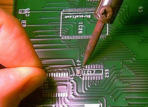
To position a chip, lay it on top of the corresponding imprint on the board. With your solering iron, briefly touch the bottom right and the upper left pin, for about 1 second. This should melt the small amount of solder coating the board, and "anchor" the chip in place. Realize that the chip is not properly soldered yet: all we did was to hold it in place. N.B. if you made your board yourself, or if you ordered a gold-coated board, you'll have to deposit a minute amount of solder on these two pads before you install the chip.
Make sure the chip is properly aligned. The easiest way is to illuminate the board from under: you will immediately see if the pins are properly sitting on the pads. Do not satisfy yourself with anything less than 100% perfect alignement. At this point it's very easy to correct mistakes: touch the anchored pin(s) with the soldering iron to melt the solder, and move the chip. Once it's fully soldered, missalignements become a nightmare, so take your time. This is especially true for the ISP1161 chip: make sure all four sides are absolutely perfectly aligned.
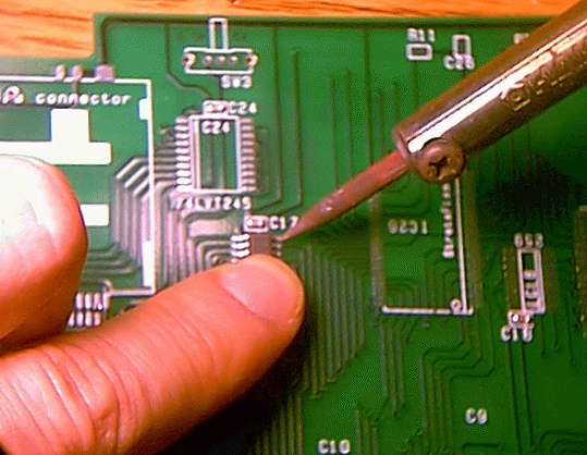
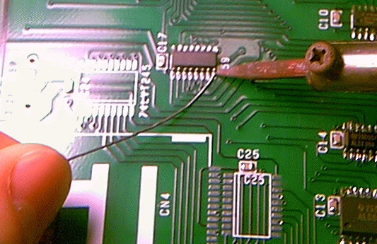
For the '74ALS' series and memory chips, my favorite method is place the solder wire along the right side of the chip, touching all the pins. The end of the wire should be flush with the last pin. Touch this last pin with your soldering iron: this will cause the solder to melt upto the next pin. Briefly touch your iron to the pad in front of the first pin, to ensure that the solder will flow on both the pin and the pad. Then repeat this "chewing away" procedure with the second pin, the third, etc, finishing with the one you have anchored. Repeat the process on the other side. With a bit of practice, soldering a chip in this way takes less than a minute (but don't rush it: this is not a race).
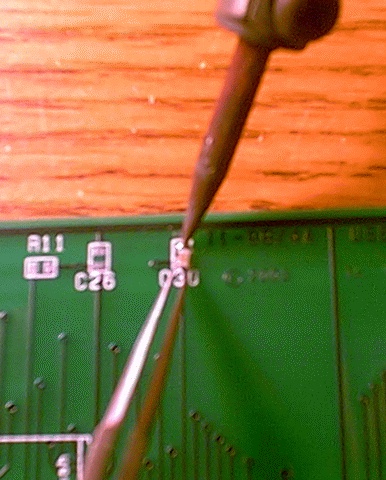
For the minuscule resistors and capacitors, I find it easier to deposit a clump of solder on one pad, to grab the component with tweezers, and to shove one end into the molten solder. Then solder the other end as described above. Finally, come back to the first end, and touch your soldering iron the the point where the component meets the pad. You will note that there is a 100 nF cap very close to each chip, I found it easier to solder the cap first, then the chip.
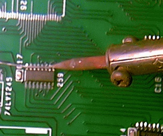
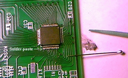
Soldering the ISP1161 is a bit more difficult, because the pins are so close that solder bridges tend to appear frequently. This is why it's nice to have really narrow solder coils. Another solution is to use solder paste: since it's applied cold, you can always wipe away any excess. Then you melt it by touching each pin with the soldering iron, at the point where it contacts the pad. Note that Radio Shack sells solder paste (not Kester's) for a more reasonnable price than Digikey...
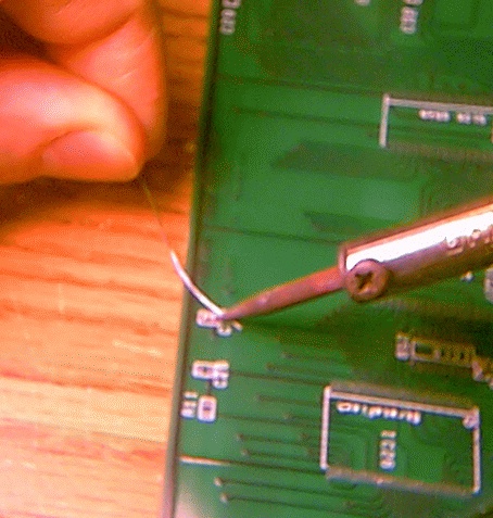
When installing the connectors and switches, you will note that they have little "tabs" that should be insert into dedicated holes in the PCB, then folded down. This is meant so that mechanical stress is not applied to the electrical connections. Make very sure that folding these tabs does not place them in contact with a signal trace (you may have to bend some outwards, e.g. for the USB-A connector). Just to be on the safe side, I also soldered each tab to its hole. The SmartMedia connector has two plastic knobs that must fit into two small holes in the PCB. Make sure you also solder the large pins at the front: this will provide additional stability.
Once the component is soldered, you must check that is was properly done. There are two potential problems: no-connects and solder bridges.
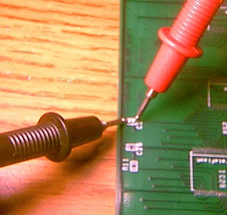
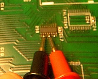
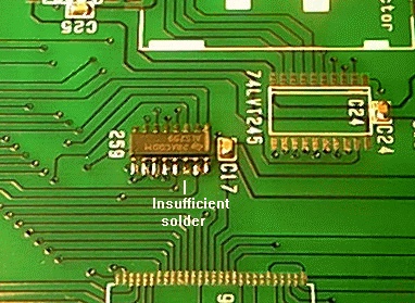
In a no-connect, the solder wasn't properly spread on both the pin and the pad (or it wasn't hot enough) and it does not make contact. To detect these, take a continuity tester (a function available in most multimeters) and touch one electrode to the top of the pin, the other to the pad, away from the solder. If there is a no-connect, you can often solve the problem by just touching your soldering iron to the point where the pin meets the pad. Sometimes, you may have to add a bit of solder.
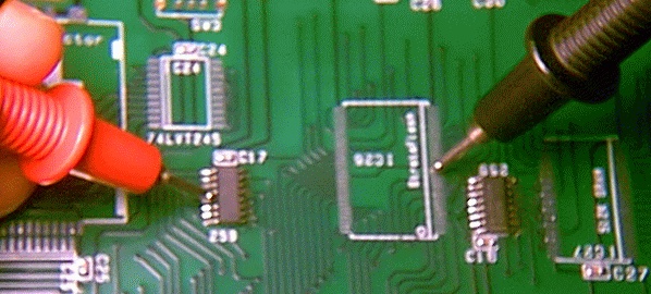
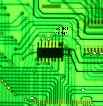
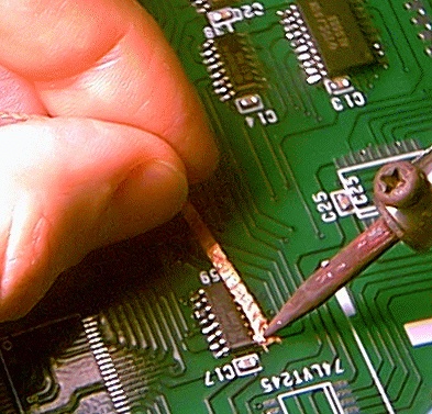
Solder bridges form when there was too much solder and it formed a bead in between adjacent pins. These are easy to detect by transparency, holding the board in front of a light source. You can also use the continuity tester, but be aware that some adjacent pins may be connected to the same signal by design. So if you don't see any apparant bridge, check the schematics. To clear a solder bridge, place the desoldering braid over it, then touch your soldering iron to the braid for 2-3 seconds on top of the bridge: the braid should "drink" the excess solder. Make sure you didn't create a no-connect in the process...
When installing capacitors, be aware that all the 100 pF are installed in the same manner, across the power supply lines. So it is critical that you check for shortcuts every time you solder one of these. If you solder them all and then do the check, you will never know which one is the culprit! In fact, as a general rule, check each chip while installing it.
Click on any image to enlarge it.
|
Deposit a blob of solder on one pad. |
Position the cap in the molten solder. |
Put solder on the other side (or both). |
Check for shortcuts. |
|
Deposit the barest amount of solder on top right pad. |
Position the chip while melting solder on this pad. |
Verify alignment with back light. |
Solder bottom left pad. |
|
Solder all other pads. |
Check for shortcuts (also check with back light). |
Check for connection (of course, it helps to know which goes where...). |
|
No connect. |
Solder bridge (shortcut). |
Removing a bridge with desoldering braid. |
The principle is the same as for TTL chips: deposit solder on one pad, anchor the chip in it, verify the alignment (tip: use a light table), then solder the opposite pad. Soldering the remaining pins is made easier by using solder paste, as you can better control the amount: you need very little.
|
A makeshift light table |
Depositing very little solder paste |
My suggestion is that you build the board stepwise and check it after each step.
First, get into the proper mindset: this is gonna be a lot of fun, so don't rush it. There is no need to finish your board in one afternoon, not even in one week-end (although it's feasible). So take your time, put on some soft music, and take frequent breaks. I know it's adictive ("Ok, just one more chip and I stop"), but it's better to take a pause long before you back aches, your eyes burn or your hands begin to shake. If you're the kind who enjoys building model galleons or solving 2000-piece jigsaw puzzles, you know what I mean.
Second, get the proper tools. There is nothing like inadequate tools to turn a heap of fun into a complete nightmare. You need good tweezers, I don't care how much you have to pay for these: you need them. You also need eutectic, narrow coil solder and a decent soldering iron. A strong magnifier, preferably with a stand, will help a lot. And you also need a continuity tester, or a multimeter with such a function.
Now, let's get started: To be on the safe side, begin each test by removing all cards from your PE-box, including the connection card (you'll need to remove a screw at the back of the PE-box to free that one).
First, install only the voltage regulators (Q1, Q2), the 47 uF capacitor (C46), and the 100 nF caps that are near the regulators (C34, C35). Also install the heat sink (HS1), preferably using heat-conducing paste.
Then place the card in the PE-box and turn power on for 3 seconds. Turn power-off and verify that the regulators are not hot. Turn power on again, for a minute or two. Make sure there is no smoke, nor "burnt" smell. During that time, verify the voltages. You can place the negative electrode of your voltmeter on the bottom plate of the PE-box. A convenient place to test the voltage is where the voltage-selection switch for the SmartMedia card (SW3) will be. The connections are even labelled "+5V" and "3.3V" over there.
Install the four 74ALS245 (IC1, IC2, IC3, IC4), the 74ALS688 (IC13), the adjacent 74ALS138 (IC14), the first 74ALS259 (IC16), their respective 100 nF caps (C1,C2,C3, C4, C13, C14, C16), the main LED (LED1) and its 470 Ohms resitor (R1), the DIP-switch (SW1, all switches open) and its 4.7K resistor network (R14, it looks like a chip, only pale blue).
Again, place the card in the PE-box and turn power on for a short time: none of the chips should become hot. Now you can put the connection card back in place, then power-up your PE-box and your console. Using a debugger such as the MiniMemory's EasyBug, toggle CRU bit 0 at address >1F00: the LED should shine.
For the next step, install the remaining 74ALS chips (including their 100 nF caps), the master switch (SW2), the three memory chips (IC26, IC27, IC28) and the pull-up resistors for the Flash-EEPROM (R11 = 4.7K, R12 = 47K). Leave the USB controller and its circuitery for later, ditto for the Smartmedia circuitery and its 74LVT245 chips.
Again, do a smoke test before you connect your console. Make sure the master switch is toggled to the ground ("TI" position) and SW4 towards the "TI" position (unless you're using a Geneve, of course). Toggle CRU bit >1F00 until the LED shines, then access memory at >4000. The StrataFlash should read as >FF all the way to >4FFF, then random values will appear in the SRAM domain at >5000 to >5FFF.
Make sure you can write anything you want at >5000 and above, indicating that the SRAMs are ok. Then write >90 at >4001, this places the StrataFlash in "read chip ID" mode, and you should read back the manufacturer code (>89), chip ID, etc. Writing >FF at an odd-numbered address should return the EEPROM to standard reading mode.
You may also want to write arbitrary data to the area >5FF0-5FFF. Then set CRU bit >1FF2 to 1: your values should disappear because this area now maps to the still-missing ISP1161.
Next, install the SmartMedia connector (CN4), the two 74LVT245 buffers (IC24, IC25) and their bypass caps (C24, C25), the 1.5K pull-up resistors (R3 to R6) and the voltage selection switch (SW3).You don't need the switch if you intend to use only 3.3 volts cards. In this case, solder a piece of wire between the middle switch hole and the left one (labelled 3.3V).
Try and read back CRU bits >1FFA and see if it toggles when there is a SmartMedia card into the connector. The golden contacts on the SmartMedia card should face the board when the card is inserted (i.e. the left of the PE-box).
Then set CRU bits >1FF0 and >1FF2 to 1, and CRU bit >1FF4 to '0'. Write >70 at address >4FFC: you should read something like >C0 at >4FF0.
Finally, install the ISP1161 chip (IC29): by now you should have a lot of experience with soldering, but see above for soldering tips with this extra-small chip. Also install the USB connectors (CN2, CN3), and all the remaining components: MOSFET (Q3), resistors, capacitors, crystal (XTAL1), etc. The second LED (LED2) is optional, so is the 1.5K pull-up to 3.3 volts (R7).
To test the chip, set CRU bits >1FF0 and >1FF2 to '1' then write >B5 at address >5FFF. You should read >61 out of 5FF4.
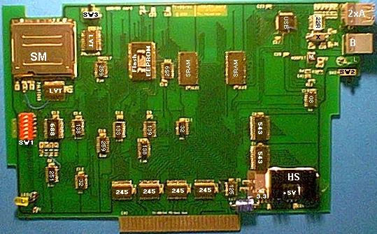
Here is a picture of the final product, version 1.5. If you are curious, I also have a picture of version 1.1, here.
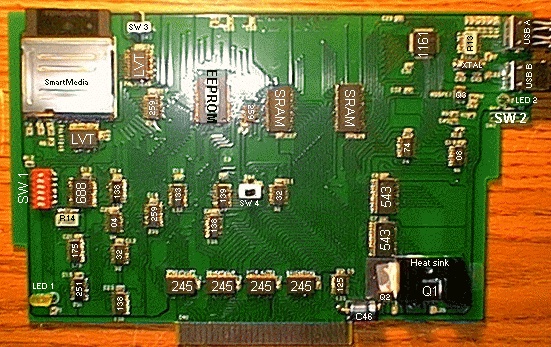
1161: ISP1161 USB controller.
EEPROM: StrataFlash 8 megabytes (upside down).
SRAM: Two 512 Kbytes SRAM (upside down).
688: 74ALS688 comparator, 8 bits.
543: 74F543 registered transceivers (2).
259: 74ALS259 addressable latch (3 for CRU output. One is upside
down).
251: 74ALS251 encoder 8-to-1 (CRU input).
245: 74ALS245 transceivers (4).
175: 74LAS175 quad latch.
139: 74ALS139 dual decoder 2-to-4.
138: 74ALS138 decoder 3-to-8 (3).
133: 74ALS133 NAND gate, 13 inputs.
125: 74LS125 tri-state buffer.
74: 74LAS74 duad flip-flop.
32: 74ALS32 quad OR gates (2).
08: 74LAS08 duad AND gates.
04: 74LAS04 hex inverters.
LVT: 74LVT245 transceivers, 3.3 volts (2).
Q1: voltage regulator, +5 volts.
Q2: voltage regulator, +3.3 volts.
Q3: dual MOSFET.
XTAL: Crystal, 6 MHz
LED1 and 2: Light emmiting diodes.
R13: Resistor network, 7x 22 ohms
R14: Resistor network, 7x 4.7 kiloOhms
SW1: 6x DIP-switch (CRU address, write protections)
SW2: SP3T switch (TI-99/4A / Geneve / Off).
SW3: SPDT switch (SmartMedia voltage: 5 / 3.3 volts)
SW2: DPDT switch (TI-99/4A / Geneve ).
USB A: Two USB downstream ports.
USB B: One USB upstream port.
SmartMedia: SmartMedia card connector.
IC1: 74ALS245
IC2: 74ALS245
IC3: 74ALS245
IC4: 74ALS245
IC5: 74LS125
IC6: 74F543
IC7: 74F543
IC8: 74ALS138
IC9: 74ALS139
IC10: 74ALS133
IC11: 74ALS32
IC12: 74ALS32
IC13: 74ALS688
IC14: 74ALS138
IC15: 74ALS251
IC16: 74ALS259
IC17: 74ALS259
IC18: 74ALS259
IC19: 74ALS08
IC20: 74ALS04
IC21: 74ALS175
IC22: 74ALS74
IC23: 74ALS138 (Geneve)
IC24: 74LVT245
IC25: 74LVT245
IC26: StrataFlash DA28F640J5A150
IC27: 512K SRAM (e.g. M68Z512W-70NC)
IC28: 512K SRAM
IC29: USB controller ISP1161
Q1: 5V voltage regulator TL780-05CKTER
Q2: 3.3V voltage regulator UA78M33CDCYR
Q3: Double MOSFET ZXMP3A17
SW1: 6x DIP switch
SW2: SP3T switch
SW3: SPDT switch
SW4: DPDT switch
XTAL1: 6 MHz crystal, 18 pF
C1 to C35: ceramic capacitors 100 nF
C36 to C41: ceramic capacitors 47 pF
C42,C43: ceramic capacitors 18 pF
C44,C45: ceramic capacitors 1 nF
C46: electrolytic capacitor 47 uF
R1,R2: resistors 470 Ohms
R3 to R9: resistors 1.5 kOhms
R10, R11: resistors 4.7 kOhms
R12: resistor 47 Kohms
R13: resistor network, 7 x 22 Ohms
R14: resistor network, 7 x 4.7 kOhms
CN2: 2x USB-A connector
CN3: USB-B connector
CN4: SmartMedia connector
LED1: Amber light-emiting diode
LED2: Any color you fancy
HS1: Heat sink
Revision 1. 6/24/03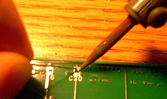